Ide Pcb Note 8, Skema Pcb
Ide Pcb Note 8, Skema Pcb. Dalam dunia skema pcb mungkin Anda pernah mendengar dengan yang namanya kumpulan skema pcb. Komponen dasar skema pcb beserta fungsi dan simbolnya yang harus kamu ketahui, Simak ulasan terkait skema pcb dengan artikel Ide Pcb Note 8, Skema Pcb berikut ini
![Samsung Galaxy Note 8 0 N5100 Charging Port PCB Board Samsung Galaxy Note 8 0 N5100 Charging Port PCB Board](https://www.cellspare.com/image/cache/data/Samsung/Charging20Socket/galaxy-note-8.0-n5100-charging-port-pcb-board-module-opt-500x500.jpg)
Samsung Galaxy Note 8 0 N5100 Charging Port PCB Board Sumber : www.cellspare.com
![Samsung Note 8 SM N950U Pcb Layout Teardown Samsung Note 8 SM N950U Pcb Layout Teardown](https://blogger.googleusercontent.com/img/b/R29vZ2xl/AVvXsEi16H1M5LtiHETbPcS9OHxT0QU8kW0TF2v0HgA0qX7CZPONyshHcbRl55sJaaRDWNr_NcffqmTBYD3xFWHnFXrWdYz-fjmmJmE1IvnFlIgdebhvUK5Jyp_zltvLkbq7cYlPDSbHF1KADTTR/w1200-h630-p-k-no-nu/n950u.jpg)
Samsung Note 8 SM N950U Pcb Layout Teardown Sumber : mobil1tech.blogspot.com
![Xaiomi Mi Note 3 Charging Problem Solution Repair Ways Xaiomi Mi Note 3 Charging Problem Solution Repair Ways](https://blogger.googleusercontent.com/img/b/R29vZ2xl/AVvXsEgnKb2vqGnbEa4joxBvO0BvVPX_Wn9WhV6RLxBXmISNJetwSXeRHuox15RhVm4qrB0PQukdwdRPZ5rYjK7dL5OX7Ngnj0hJpRaYUvpFhCSC1F8enjAixFYSEXGw48O-X2PJiKygydnPfm8/s640/Xiaomi_mi_note_3_charging_pcb_connector.png)
Xaiomi Mi Note 3 Charging Problem Solution Repair Ways Sumber : iphoneharwarerepairing.blogspot.com
![PCB Main Board for Samsung Galaxy Note N7000 PCB Main Board for Samsung Galaxy Note N7000](https://cdn2.bigcommerce.com/server5800/8c4e0/images/stencil/500x659/products/3883/10057/samsung_i9100_pcb_main_board_01__71977.1355451631.jpg?c=2)
PCB Main Board for Samsung Galaxy Note N7000 Sumber : www.parts4repair.com
![Samsung Galaxy Note 4 Repair iFixit Samsung Galaxy Note 4 Repair iFixit](https://da2lh5cs8ikqj.cloudfront.net/cart-products/hJDjxYaKp6TXM2EI.standard)
Samsung Galaxy Note 4 Repair iFixit Sumber : www.ifixit.com
![OtterBox Commuter for Galaxy Note 4 5 8 9 Green Circuit OtterBox Commuter for Galaxy Note 4 5 8 9 Green Circuit](https://distinctinkimages.com/comnote5black/p553.jpg)
OtterBox Commuter for Galaxy Note 4 5 8 9 Green Circuit Sumber : www.ebay.com
![Samsung Galaxy S8 Plus Service Manual SM G955F Service Samsung Galaxy S8 Plus Service Manual SM G955F Service](https://notebookschematics.com/wp-content/uploads/2017/06/G955F-service-Manual-2-300x194.jpg)
Samsung Galaxy S8 Plus Service Manual SM G955F Service Sumber : notebookschematics.com
![PCB Main Board for Samsung Galaxy Note N7000 PCB Main Board for Samsung Galaxy Note N7000](https://cdn2.bigcommerce.com/server5800/8c4e0/images/stencil/500x659/products/4990/11900/samsung_n7100_main_board_02__38744.1363166692.jpg?c=2)
PCB Main Board for Samsung Galaxy Note N7000 Sumber : www.parts4repair.com
![Samsung Galaxy Note8 Teardown iFixit Samsung Galaxy Note8 Teardown iFixit](https://d3nevzfk7ii3be.cloudfront.net/igi/hdqmO1Mo1Y2BK4bx.full)
Samsung Galaxy Note8 Teardown iFixit Sumber : www.ifixit.com
![OEM Samsung Galaxy Note 8 N5110 N5100 Charge Port PCB OEM Samsung Galaxy Note 8 N5110 N5100 Charge Port PCB](https://cdn8.bigcommerce.com/s-xaru2divgn/images/stencil/2000x2000/products/2738/9252/Smn5110chg1-2__37336.1513013357.jpg?c=2)
OEM Samsung Galaxy Note 8 N5110 N5100 Charge Port PCB Sumber : globaldirectparts.com
![OEM ASUS M80TA VIVOTAB NOTE 8 TABLET REPLACEMENT 64GB OEM ASUS M80TA VIVOTAB NOTE 8 TABLET REPLACEMENT 64GB](https://lh3.googleusercontent.com/blogger_img_proxy/AEn0k_vc9VMIrt6vR2uJDIgJb5CsSMcQD2NpT3fbVq03DvGG8STFaZDQtsKJlS8WD2tUBJUL-SavEWQfQzx8IozFbNRC1Lqac2ih3-ZavfRlc7Vj8muj6am9pzR7Vrf2esX04Q=s0-d)
OEM ASUS M80TA VIVOTAB NOTE 8 TABLET REPLACEMENT 64GB Sumber : www.ebay.com
![Samsung Note 8 SM N950U Pcb Layout Samsung Note 8 SM N950U Pcb Layout](https://i.imgur.com/Mbrqf8J.jpg)
Samsung Note 8 SM N950U Pcb Layout Sumber : forum.gsmdevelopers.com
![Samsung S8 Schematic PDF Free Manuals Samsung S8 Schematic PDF Free Manuals](https://image.jimcdn.com/app/cms/image/transf/dimension=620x10000:format=jpg/path/sf448448cbeeed0ff/image/i7ce82573f38668dc/version/1524248346/image.jpg)
Samsung S8 Schematic PDF Free Manuals Sumber : www.gadget-manual.com
![OEM Samsung Galaxy Note 8 i467 N5110 N5100 Vibe Motor OEM Samsung Galaxy Note 8 i467 N5110 N5100 Vibe Motor](https://cdn8.bigcommerce.com/s-xaru2divgn/images/stencil/2000x2000/products/2664/9170/Smi467mtr1-2__16687.1513009626.jpg?c=2)
OEM Samsung Galaxy Note 8 i467 N5110 N5100 Vibe Motor Sumber : globaldirectparts.com
![Generic Dock Charging PCB Board for Xiaomi Redmi Note 3 Generic Dock Charging PCB Board for Xiaomi Redmi Note 3](https://cdn7.bigcommerce.com/s-8c4e0/products/11324/images/33618/redmi_note_3_dock_charging_pcb_board_01__83114.1456498261.380.380.jpg?c=2)
Generic Dock Charging PCB Board for Xiaomi Redmi Note 3 Sumber : www.parts4repair.com
![Samsung Galaxy Note 8 0 N5100 Charging Port PCB Board Samsung Galaxy Note 8 0 N5100 Charging Port PCB Board](https://www.cellspare.com/image/cache/data/Samsung/Charging20Socket/galaxy-note-8.0-n5100-charging-port-pcb-board-module-opt-500x500.jpg)
Samsung Galaxy Note 8 0 N5100 Charging Port PCB Board Sumber : www.cellspare.com
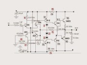
AN0159V4 Recommended PCB Pad Layouts for 8 USON 8
APPLICATION NOTE Recommended PCB Pad Layouts for 8 USON 8 WSON Packages P N AN0159 1 Ver 4 May 09 2020 1 Introduction This application note specifies the recommended Printed Circuit Board pad layouts for the following 8 USON and 8 WSON packages
![Samsung Note 8 SM N950U Pcb Layout Teardown Samsung Note 8 SM N950U Pcb Layout Teardown](https://blogger.googleusercontent.com/img/b/R29vZ2xl/AVvXsEi16H1M5LtiHETbPcS9OHxT0QU8kW0TF2v0HgA0qX7CZPONyshHcbRl55sJaaRDWNr_NcffqmTBYD3xFWHnFXrWdYz-fjmmJmE1IvnFlIgdebhvUK5Jyp_zltvLkbq7cYlPDSbHF1KADTTR/w1200-h630-p-k-no-nu/n950u.jpg)
Samsung Note 8 SM N950U Pcb Layout Teardown Sumber : mobil1tech.blogspot.com
Samsung Galaxy Note8 Teardown iFixit
15 09 2020 The Note7 came in hot but went out in a show of flames and combustion Rising out of its ashes is Fawkes the Note8 Samsung has pulled out all the stops on the specs of this phone and added a few stops where the battery s concerned Join us and hopefully not the local fire department as we open up the Samsung Galaxy Note8
![Xaiomi Mi Note 3 Charging Problem Solution Repair Ways Xaiomi Mi Note 3 Charging Problem Solution Repair Ways](https://blogger.googleusercontent.com/img/b/R29vZ2xl/AVvXsEgnKb2vqGnbEa4joxBvO0BvVPX_Wn9WhV6RLxBXmISNJetwSXeRHuox15RhVm4qrB0PQukdwdRPZ5rYjK7dL5OX7Ngnj0hJpRaYUvpFhCSC1F8enjAixFYSEXGw48O-X2PJiKygydnPfm8/s640/Xiaomi_mi_note_3_charging_pcb_connector.png)
Xaiomi Mi Note 3 Charging Problem Solution Repair Ways Sumber : iphoneharwarerepairing.blogspot.com
DesignSpark PCB Version 8 1 Has Been Released
27 02 2020 DesignSpark PCB Version 8 1 Has Been Released Note Properties for copper pouring will be taken from the Design Technology dialogue and Rules page Changes to Area Properties PCB Copper Pour Areas Below shows the Properties dialogue for Copper Pour Areas This has been implemented to allow for the expanded controls for thermal rules per
![PCB Main Board for Samsung Galaxy Note N7000 PCB Main Board for Samsung Galaxy Note N7000](https://cdn2.bigcommerce.com/server5800/8c4e0/images/stencil/500x659/products/3883/10057/samsung_i9100_pcb_main_board_01__71977.1355451631.jpg?c=2)
PCB Main Board for Samsung Galaxy Note N7000 Sumber : www.parts4repair.com
Polychlorinated biphenyl Wikipedia
A polychlorinated biphenyl PCB is an organic chlorine compound with the formula C 12 H 10 x Cl x Polychlorinated biphenyls were once widely deployed as dielectric and coolant fluids in electrical apparatus carbonless copy paper and in heat transfer fluids
Samsung Galaxy Note 4 Repair iFixit Sumber : www.ifixit.com
Xiaomi Redmi Note 8 Pro In Depth Full Bangla Review
13 09 2020 Redmi Note 8 Pro is a most awaited phone from Xiaomi After its launch we brought you the full and in depth Bangla review of this phone It has 64 Mp
![OtterBox Commuter for Galaxy Note 4 5 8 9 Green Circuit OtterBox Commuter for Galaxy Note 4 5 8 9 Green Circuit](https://distinctinkimages.com/comnote5black/p553.jpg)
OtterBox Commuter for Galaxy Note 4 5 8 9 Green Circuit Sumber : www.ebay.com
Printed circuit board Wikipedia
A printed circuit board PCB Cut through a SDRAM module a multi layer PCB Note the via visible as a bright copper colored band running between the top and bottom layers of the board Multi layer printed circuit boards have trace layers inside the board This is achieved by laminating a stack of materials in a press by applying pressure
![Samsung Galaxy S8 Plus Service Manual SM G955F Service Samsung Galaxy S8 Plus Service Manual SM G955F Service](https://notebookschematics.com/wp-content/uploads/2017/06/G955F-service-Manual-2-300x194.jpg)
Samsung Galaxy S8 Plus Service Manual SM G955F Service Sumber : notebookschematics.com
Charging Port PCB Board for Xiaomi Redmi Note 8 Pro
Xiaomi Redmi Note 8 Pro Charging Port PCB Board replacement is used to replace your damaged and not working dock port This new usb board replacement may be the part you need
![PCB Main Board for Samsung Galaxy Note N7000 PCB Main Board for Samsung Galaxy Note N7000](https://cdn2.bigcommerce.com/server5800/8c4e0/images/stencil/500x659/products/4990/11900/samsung_n7100_main_board_02__38744.1363166692.jpg?c=2)
PCB Main Board for Samsung Galaxy Note N7000 Sumber : www.parts4repair.com
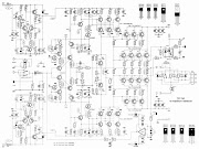
Proteus PCB Design Download 2020 Latest for Windows 10 8 7
Proteus PCB Design software combines the Schematic Capture and ARES PCB Layout programs to provide a powerful integrated and easy to use suite of tools for professional Printed Circuit Board design The Proteus PCB Design tool range is a professionals choice for modern PCB Layout With over 25 years of continuous development and innovation focus remains on adding functionality while
Samsung Galaxy Note8 Teardown iFixit Sumber : www.ifixit.com
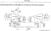
AN2409 Small Outline Integrated Circuit SOIC Package
Printed Circuit Board Guidelines AN2409 Application Note Rev 3 0 4 Freescale Semiconductor Inc 4 Printed Circuit Board Guidelines 4 1 PCB Design Guidelines and Requirements Proper PCB footprint and stencil designs are critical to ensure high surface mount assembly yields and electrical and mechanical performance of the mounted package
![OEM Samsung Galaxy Note 8 N5110 N5100 Charge Port PCB OEM Samsung Galaxy Note 8 N5110 N5100 Charge Port PCB](https://cdn8.bigcommerce.com/s-xaru2divgn/images/stencil/2000x2000/products/2738/9252/Smn5110chg1-2__37336.1513013357.jpg?c=2)
OEM Samsung Galaxy Note 8 N5110 N5100 Charge Port PCB Sumber : globaldirectparts.com
Xiaomi Redmi Note 8 Pro Charging Port PCB Board
Charging Port PCB Board for Xiaomi Redmi Note 8 Pro Smartphone 2 This part is used to replace your damaged or unworkable charging port flex cable 3 Each item has been checked and in good condition before shipping 4 The installation of any new part should be done by a qualified person We will not be responsible for any damage caused during
OEM ASUS M80TA VIVOTAB NOTE 8 TABLET REPLACEMENT 64GB Sumber : www.ebay.com
![Samsung Note 8 SM N950U Pcb Layout Samsung Note 8 SM N950U Pcb Layout](https://i.imgur.com/Mbrqf8J.jpg)
Samsung Note 8 SM N950U Pcb Layout Sumber : forum.gsmdevelopers.com
![Samsung S8 Schematic PDF Free Manuals Samsung S8 Schematic PDF Free Manuals](https://image.jimcdn.com/app/cms/image/transf/dimension=620x10000:format=jpg/path/sf448448cbeeed0ff/image/i7ce82573f38668dc/version/1524248346/image.jpg)
Samsung S8 Schematic PDF Free Manuals Sumber : www.gadget-manual.com
![OEM Samsung Galaxy Note 8 i467 N5110 N5100 Vibe Motor OEM Samsung Galaxy Note 8 i467 N5110 N5100 Vibe Motor](https://cdn8.bigcommerce.com/s-xaru2divgn/images/stencil/2000x2000/products/2664/9170/Smi467mtr1-2__16687.1513009626.jpg?c=2)
OEM Samsung Galaxy Note 8 i467 N5110 N5100 Vibe Motor Sumber : globaldirectparts.com
![Generic Dock Charging PCB Board for Xiaomi Redmi Note 3 Generic Dock Charging PCB Board for Xiaomi Redmi Note 3](https://cdn7.bigcommerce.com/s-8c4e0/products/11324/images/33618/redmi_note_3_dock_charging_pcb_board_01__83114.1456498261.380.380.jpg?c=2)
Generic Dock Charging PCB Board for Xiaomi Redmi Note 3 Sumber : www.parts4repair.com
0 Comments